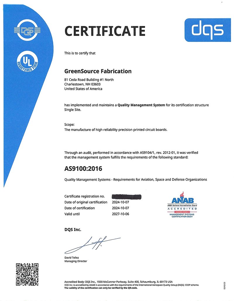
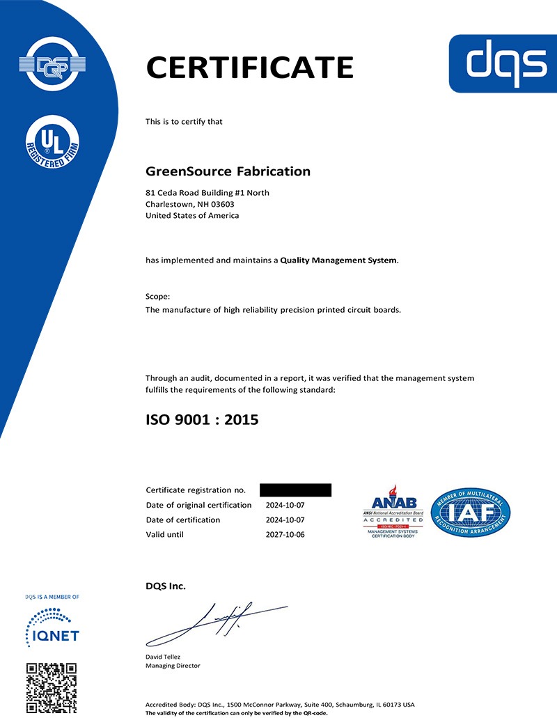
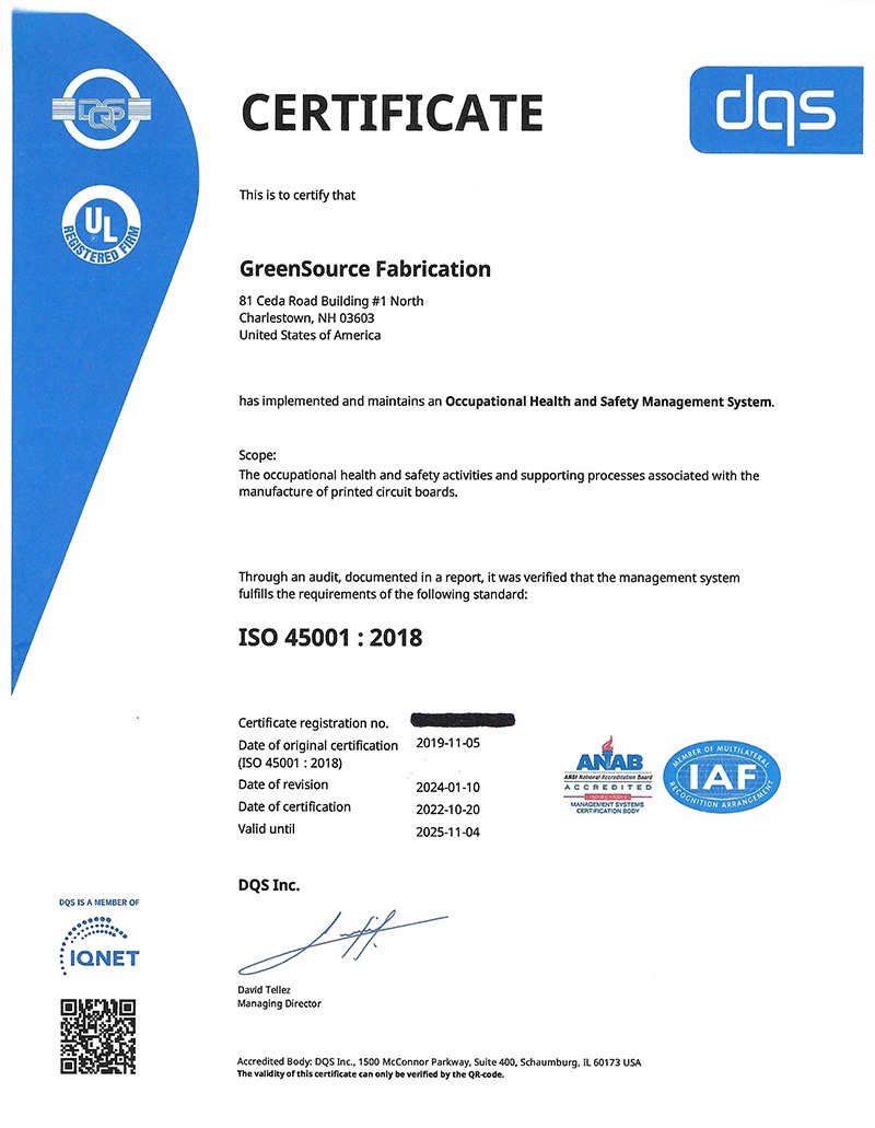
Certifications
Capabilities
At GreenSource Fabrication, we specialize in delivering 100% USA made cutting-edge solutions for the advanced HDI, UHDI and ICS markets. We expertly tackle the complexities of sub-35um features. We offer horizontal and vertical plating technologies to support sub 50um subtractive etch, mSAP, amSAP and SAP process flows to ensure every build up layer is optimized for a given design.
As you explore the detailed information on our process capabilities, you'll discover our commitment to using state-of-the-art (SOTA) equipment in every aspect of our operations. We pride ourselves on not just incorporating a few modern pieces, but ensuring that all our equipment represents the latest in technological advancements.
Pioneering in Eco-Friendly PCB Manufacturing
GreenSource Fabrication stands out as North America's first truly environmentally-conscious PCB fabrication facility. Our commitment to sustainability is demonstrated through our proprietary Aqua Regen Kinetics System (ARK) a Zero Liquid Discharge (ZLD) technology, setting a new standard in eco-friendly manufacturing processes.
Discover More About Our Capabilities
To gain a deeper insight into the breadth and depth of our capabilities, we invite you to request access to our exclusive “CAPABILITES MATRIX” section. Simply click on the button below.
For personalized assistance or more detailed information, please don't hesitate to contact us directly. We are here to address your specific needs and questions.
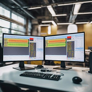 At GreenSource, our Front End Engineering and Design for Manufacturability Teams are key production steps utilized in every build. We focus on the technical requirements for the build and incorporate processes to ensure it is manufactured as efficiently as possible. Through our Design Review (DFM) and stack up modeling services, GreenSource will enable new designs to be transitioned into manufacturing with ease.
GreenSource prides itself on partnerships and will allow our product engineering teams to engage with customers early on in the design process to assure we align before projects are finalized. This allows GreenSource to develop critical Process Design Kits for product or customer specific use, which in turn, cuts down on design timelines and unexpected yield loss.
GreenSource has a dedicated NPI process where all new tools are reviewed in a structured format to reduce risk and optimize the customer experience. This robust process also allows GreenSource to take part in new cutting edge developmental projects with our customer base while clearly communicating the risks involved and the measures taken to address them.
For every project we undertake, it undergoes a meticulous review process by our FEE/DFM Team, who are tasked with designing and creating the necessary files for all manufacturing and inspection equipment required to ensure the highest quality outcome. This process is integral to supporting our Manufacturing Engineering Team and Production Team throughout every stage of the fabrication process, guaranteeing that each project is executed flawlessly from start to finish.
We use industry standard software tools; XACT PCB, Polar Speedstack, Polar SI9000 QuickSolver, Polar CGen, Frontline InCam Pro, Frontline InFlow, Frontline InSight, Frontline InCoupon, Frontline InStack, Ucamco Ucam, Ucamco Integr8tor, and Bacon Engineering.
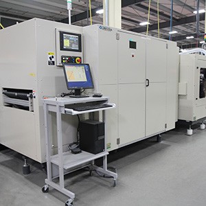 At GreenSource Fabrication, we redefine traceability in the manufacturing landscape. Traceability for us is not just a capability — it's an integral part of our commitment to excellence and innovation. It's the comprehensive tracking and documenting of every single step in our production process, from the initial raw materials to the intermediate products, all culminating in the finished product.
Central to our state-of-the-art traceability system is the use of sophisticated and individualized 2D codes assigned to each core and/or panel. These codes are seamlessly integrated with our Manufacturing Execution System (MES), enabling us to monitor the real-time location of products throughout our plant floor. This synergy of reading technology with our SCADA/MES not only facilitates real-time material tracking but also empowers the automatic selection of process-specific recipes, thereby significantly reducing the possibility of human error. Additionally, the 2D code system is instrumental in tracking vital quality information, including key product dimensions and process parameters, laying a robust foundation for the future integration of Machine Learning and Artificial Intelligence tools. This advanced tracking mechanism is more than just a navigational tool; it's the heartbeat of our operational efficiency.
Our utilization of these 2D codes extends far beyond mere tracking. They are pivotal in driving our automation and process equipment. By interacting with these codes, our machines automatically act and adjust recipe parameters, tailoring the production process to the specific needs of each product. This intelligent automation ensures unparalleled precision and customization in our manufacturing.
Furthermore, these codes are intricately linked with our quality control processes that provide a detailed record of crucial quality information, including process setpoints, laboratory analyses, and critical feature measurements. This meticulous approach ensures that every product we create at GreenSource Fabrication is not just manufactured but is fabricated with the utmost care, precision, and is tailored to deliver the best possible outcome for our customers.
In summary, our innovative use of individualized 2D codes embodies our pursuit of best-in-class manufacturing. It's a testament to our dedication of producing superior products and our commitment to ensuring customer satisfaction through unparalleled quality and precision.
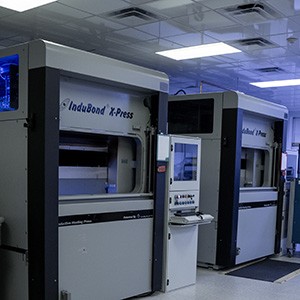 The lamination process stands at the heart of GreenSource Fabrication's printed circuit board manufacturing excellence. This intricate procedure involves the artful layering and bonding of various materials to create a unified, high-performance circuit board. During this pivotal phase, we meticulously bond together inner core layers, copper foils down to 1.5um in thickness, prepreg and glass-free bond-ply to form robust composite layer stacks. Our lamination process is finely tuned to accommodate a diverse range of materials, ensuring optimal results for every product.
The precision of our lamination process begins with the exact alignment of cores, prepreg, and foils on pins affixed to a specialized lay-up fixture. The stack is then securely bonded together using rivets or induction welding depending on the application which prevents any shift during the lamination process.
In our pursuit of excellence and accuracy, we have introduced a groundbreaking technology into our production: inductive bonding utilizing an InduBond RFX. This innovative technique offers an advanced alternative to traditional riveting for bonding the stack together. Inductive bonding enhances the precision of our panel alignment, resulting in even more accurate and reliably constructed panels.
Once prepared, the stack enters our advanced lamination presses. Governed by a sophisticated controller, the press meticulously orchestrates the lamination sequence: initiating a vacuum, precisely heating the stack, engaging the ram for optimal pressure application, and regulating a carefully controlled cooling rate.
The state-of-the-art InduBond lamination presses at GreenSource Fabrication are a marvel of technology, capable of reaching temperatures necessary for the fusion bonding of Teflon and other non-reinforced materials. What's more, the InduBond system is a testament to our commitment to sustainability, consuming 80% less energy than conventional hot oil presses. This not only enhances our efficiency but also solidifies our dedication to 'green' manufacturing practices.
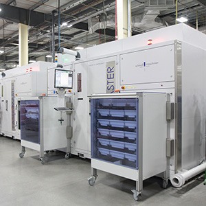 At GreenSource Fabrication, our multilayer PCB production is a symphony of precision and innovation. Essential to this process is the creation of Plated Through Holes (vias), the crucial conduits that forge connections between the various layers of a PCB. From two-layered boards to complex multilayer designs, our vias ensure seamless connectivity across all layers. This vital task is accomplished using two sophisticated methods: mechanical and laser drilling.
In our mechanical drilling operations, we have taken automation to the next level with the Schmoll Stackmaster, an automated pinup cell. This sophisticated machine expertly aligns stacks of panels prior to drilling, ensuring precise alignment. The Stackmaster further streamlines our process by loading and unloading drill modules using an Automated Guided Vehicle (AGV), significantly reducing the need for human interaction. Post-drilling, the Stackmaster skillfully de-pins and de-stacks the panels, efficiently transferring them into our cutting-edge deburr machine for a thorough cleaning. This machine employs a high-flow rinse system, meticulously cleaning the panels post-drilling to ensure the absolute removal of any residual debris in the vias. This step is crucial in maintaining the integrity and reliability of our PCBs, as even the smallest particle can compromise the functionality of the final product.
Our mechanical drilling process is a marvel of accuracy and efficiency. We employ state-of-the-art drilling modules equipped with automated optical positioning systems, which not only ensure unparalleled precision but also eliminate the need for hard tooling. This advanced optical alignment allows for greater flexibility and speed in our production processes. Outfitted with high-speed spindles, our modules are adept at handling the most demanding tasks, including the use of microtools, with remarkable ease. Quality control is further enhanced as each drill bit is managed by an automated tool changing system 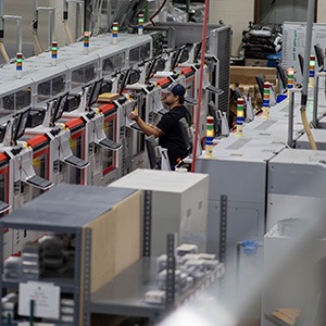 and undergoes rigorous laser inspection for length and diameter. This meticulous process guarantees the highest quality and consistency in our drilled holes, ensuring that each PCB we produce meets our exacting standards and exemplifies the pinnacle of manufacturing excellence.
However, when it comes to creating blind vias and through-vias with extremely small diameters, mechanical drilling faces limitations, primarily due to increased risk of drill bit breakage and consequent rise in scrap costs. To overcome this challenge, we harness the power of laser drilling. In the realm of laser drilling, our capabilities are equally impressive. We utilize a Combi drill that incorporates a multi-step process: a UV laser for piercing the initial layer of copper, a CO2 laser for removing glass and resin, followed by a UV cleaning step to purify the copper target pad at the hole's base. For Ultra-High-Density Interconnect (UHDI) work, we deploy the Pico drill, which utilizes a green laser pulsing in pico-seconds. This advanced technology minimizes heat generation and copper splatter, crucial for the most delicate, precise and high density drilling requirements. Both the Combi and Pico drills are fully automated, with loading and unloading capabilities that not only minimize handling but also maximize operational uptime.
This dual approach to drilling - combining the broad applications of mechanical drilling with the density achieving laser ablation technology - exemplifies our commitment to versatility and excellence in PCB manufacturing. At GreenSource Fabrication, we are dedicated to pushing the boundaries of technology to deliver products that not only meet, but exceed our customers’ expectations.
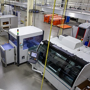 GreenSource Fabrication utilizes cutting-edge Dry-Film resist and solder mask photo-imaging technology. Our facility houses two state-of-the-art Direct-Imaging machines, each boasting the capability of achieving HDI levels of precision. For tighter tolerance and smaller featured products, GreenSource utilizes a third DI machine with the capability of achieving UHDI feature resolution.
Our advanced automation significantly minimizes operator intervention, featuring streamlined automated loading, unloading, and double-sided imaging with panel flipping. This sophisticated automation enables us to efficiently image with maximum uptime.
We have elevated our debris mitigation strategies by incorporating a touchless electrostatic cleaner. This advanced system effectively attracts and removes particulates without any physical contact, drastically reducing waste and minimizing operator interaction such as refreshing tacky roller paper. This enhancement not only fortifies the cleanliness of our imaging processes but also ensures the highest standards of quality, aligning with our commitment to innovative and sustainable practices.
Our commitment to excellence extends to eliminating human error in our imaging processes. By utilizing a sophisticated 2D barcode system, each panel is automatically identified, ensuring the selection of precise imaging parameters and operating conditions tailored for each individual panel. This innovation not only streamlines our processes but also guarantees the utmost accuracy and consistency in our production.
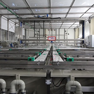 At GreenSource Fabrication, our post-drilling procedures set a new standard in the PCB manufacturing industry. Following both laser and mechanical drilling processes, we meticulously clean and prepare the hole wall surfaces for metallization. Our advanced hole preparation processes, which contribute to our consistently reliable micro-vias, are specifically designed to enhance the surface area of the hole walls, setting the stage for optimal low build copper deposition through electroless copper techniques. This foundational layer of copper is then thoroughly built up through our state-of-the-art electrolytic plating processes, which can be applied both horizontally and vertically depending on the application.
Our electrolytic capabilities are comprehensive, including through-hole filling, blind or buried microvia filling, conformal plating, and pattern plating. Each process is backed by the relentless support of our Lab and Quality Teams. We ensure the highest standards of reliability and coverage consistency, which are regularly monitored through in-situ measurements, cross-sectional analytics, and rigorous stress tests.
What truly sets GreenSource Fabrication apart, and what we continually refine for even greater excellence, is our use of panel plate technology instead of button plate. This innovative approach significantly reduces multiple potential failure points during production, enhancing both efficiency and product integrity. Moreover, our cutting-edge vertical plater is uniquely capable of handling ultra-thin, sub 50 micron, materials is a testament to our commitment to versatility and precision.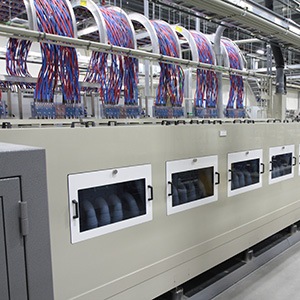
We are also pushing the boundaries in plating high aspect ratio blind vias with SAP levels of line and space, breaking new ground in PCB manufacturing capabilities. To support these diverse and demanding applications, we feature seven different electrolytic plating baths, each specifically designed to cater to different copper plating requirements.
At GreenSource Fabrication, we are not just manufacturing PCBs; we are redefining the possibilities of the PCB industry through innovation, precision, and a relentless pursuit of perfection.
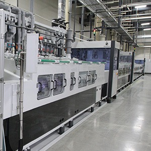 At GreenSource, we pride ourselves on our multi-pronged approach to circuit creation, featuring Direct Image Print-and-Etch (DIPAE) methodology alongside our cutting-edge mSAP and amSAP process flows. The choice of process is meticulously tailored to each technology challenge presented, which ensures optimal end results. Our diverse processing capabilities enable us to seamlessly adapt and select the most effective solution for any project.
Our advanced chemical technologies set new industry standards for safety and precision. We employ low-free-acid etching solutions, significantly enhancing operator safety while simultaneously ensuring exceptionally sharper side walls compared to traditional high-acid solutions. Moreover, our alkaline etching technology is specially optimized for superior processing of resistor materials and solderable surfaces.
In synergy with our state-of-the-art imaging technology, these processes empower us to achieve UHDI levels of resolution, a testament to our relentless pursuit of excellence. Looking ahead, we are excited about the development of integrating in-house developed automation into our SAP process flow for ICS fabrication.
This initiative promises to further elevate our capabilities and reinforce our position at the forefront of the industry.
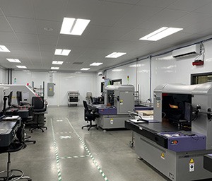 GreenSource Fabrication uses cutting edge technologies to ensure product conformity while still in process, well before the product reaches final testing. Performing in-situ inspection enables faults to be detected directly following specific processes or a set of processes, to verify the integrity of the circuitry before continuing.
Automated Optical Inspection (AOI), a non-destructive quality inspection step for our products, allows us to find critical faults on the board such as opens, nicks, protrusions, shorts, and over/under etched lines, at various process stages. When critical defects are found, Automated Optical Shaping (AOS) can be used to repair these types of defects, with customer approval.
Alongside our state-of-the-art optical inspection equipment, we also use advanced measurement technologies. Confocal microscopy delivers highly accurate measurement data and can precisely measure feature shape, height, depth, and surface roughness.
We also deploy a semi-automated video measuring system which is able to achieve non-contact automatic measurements and can precisely detect small gaps at a low magnification enabling the measurement of complex three-dimensional surfaces. This gives us the capability for quick precise automated measurements of critical features.
In addition to our in-process product inspection, we utilize state-of-the-art laboratory equipment such as automated titration, ICP, and CVS analysis to ensure the quality of our chemical lines. Every chemical bath in the facility is analyzed daily, with data recorded and plotted to continuously monitor and ensure processes are in control. Line controls, automated dosing, and operational parameters can be viewed and adjusted if needed, directly from the laboratory computers. This allows for our staff to make hands-free chemical adjustments efficiently and safely without ever leaving the lab.
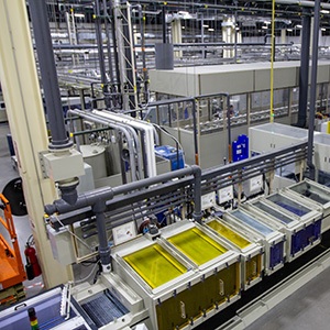 At GreenSource Fabrication, our strategic partnerships with key suppliers have enabled us to offer an array of advanced surface finish technologies, each tailored to meet the evolving demands of the industry.
ENIG: Our automated Electroless Nickel Immersion Gold (ENIG) line is a testament to our commitment to flexibility and efficiency. It is adept at handling standard technology work with remarkable speed, while also catering to complex designs with tight dams. Our state-of-the-art process, enhanced with advanced chemistry, ensures effective treatment in critical areas, preventing issues like 'nickel wall growth' and guaranteeing superior surface quality.
HASL: The automated Hot Air Solder Leveling (HASL) process at GreenSource is a model of precision. Utilizing finely tuned air knives, we ensure a consistently desired coating, a crucial factor in achieving the highest quality and reliability in our PCBs.
As part of our comprehensive services, we currently engage contract services for a variety of specialized finishes, including Electroless Nickel Electroless Palladium Immersion Gold (ENEPIG), Electroless Palladium Autocatalytic Gold (EPAG), Immersion Silver, Immersion Tin, Organic Solderability Preservatives (OSP), Lead-Free HASL, and electrolytic nickel-gold (soft gold) for wire bonding as well as electrolytic nickel-gold (hard gold) for high wear mechanical interfaces.
Looking to the future, our technology chart is ambitiously set to expand our in-house capabilities. We are targeting to bring ENEPIG, Immersion Silver (IS), and electroplated nickel-gold processes into our facility in the near future. This expansion is a reflection of our continuous pursuit of technological advancement and our commitment to providing a comprehensive range of high-quality, cutting-edge surface finish options to our clients.
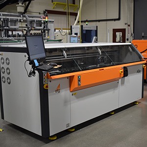 GreenSource Fabrication utilizes cutting-edge electrical test technologies through the use of Flying Probe Testers which check the electrical continuity and isolation of each and every board. Our four flying probe machines test with incredible speed allowing us to test very complex and very dense designs with ease. Two of our four machines are fully automated which load and unload panels or PCBs as well as sort parts which contain defects from those which do not. These testers also have the capability to do Latent, Kelvin, and Hipot tests. We also utilize Vitrek high voltage units for Hipot testing.
GreenSource utilizes their in-house owned CAT-OM tester to perform IPC required resistance testing. This ensures that our boards can withstand the stress of component soldering to help minimize latent defects. GreenSource routinely tests “D” coupons well in excess of the IPC standard of six (6) thermal cycles to guarantee the accuracy and consistency of our processes.
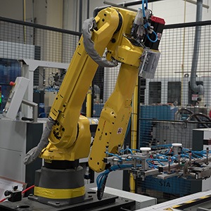 GreenSource Fabrication stands at the forefront of technological innovation, proudly recognized as one of the most automated PCB manufacturers in North America. Our cutting-edge automation equipment, expertly supplied by our sister company, GreenSource Engineering, sets a new standard in the industry.
Our advanced automation suite includes state-of-the-art loaders and unloaders equipped with slipsheeting and touchless centering capabilities, which are meticulously designed for uninterrupted operation and minimal human intervention. Our turn stations, designed to maintain orientation, include fault buffers which respond proactively to upstream process failures, and flexible buffers which respond for optimal cooling or set holding times, exemplify our commitment to seamless efficiency.
We also boast an array of bespoke automation solutions, such as a dedicated raw material loader for our automated Stackmaster cell and in-line legend automation, each designed for specific tasks in mind.
Our sophisticated SCADA and MES systems are the backbone of our operational excellence, maximizing equipment efficiency and alerting our production and maintenance teams to any concerns with equipment or products. This centralized visualization and control across various levels — Plant, Area, Line, or Cell — enable unparalleled oversight and efficiency, allowing us to achieve more with less. These systems are pivotal in real-time data collection from equipment, facilitating the calculation of key process indicators like Overall Equipment Effectiveness (OEE) and Total Effective Equipment Performance (TEEP), ensuring we remain at the cutting edge of PCB manufacturing.
Enhancing these capabilities, our SCADA/MES systems are seamlessly integrated with our Enterprise Resource Planning (ERP) system. This integration allows for optimized process loading and enhanced queue visualization within the SCADA framework, further streamlining our operations. Additionally, our Lab Management System is connected to the SCADA/MES, enabling the MES to determine if a process has been analyzed within the appropriate time window. This feature allows for real-time visualization within the SCADA system and notifies technicians if a process has received authorization to proceed.
Crucially, our SCADA/MES is based on the Unified Namespace (UNS), positioning it as the single source of truth within our organization. This design is instrumental in facilitating data-driven decision-making, ensuring that every step we take is informed, precise, and strategically aligned with our goal of remaining at the forefront of the PCB manufacturing industry.
At GreenSource Fabrication, our commitment to automation, underpinned by our sophisticated SCADA/MES system, is more than just a feature — it's a promise to deliver unmatched efficiency, precision, and quality in every PCB we produce.

